
Context:
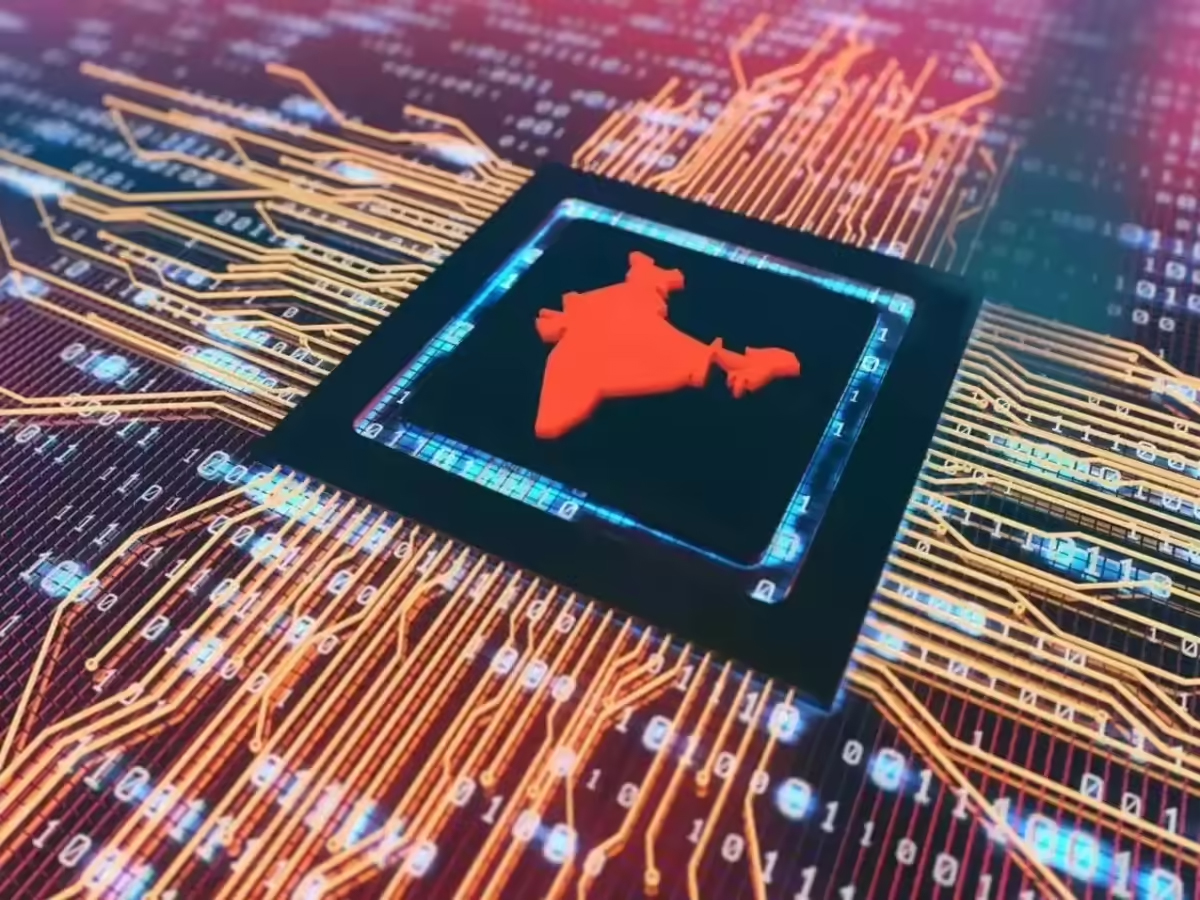
Recently, the Central Government approved two new semiconductor projects under the India Semiconductor Mission (ISM). These include the country’s first Gallium Nitride (GaN)-based semiconductor and Micro-LED manufacturing facility at Dholera, Gujarat, and a new semiconductor packaging and testing facility in Surat. With these approvals, the number of projects sanctioned under the Semiconductor Mission has reached 12. Additionally, Tata Electronics and the Dutch company ASML have signed a technology collaboration agreement for India’s first chip fabrication facility.
These developments indicate that India no longer wants to remain merely a consumer market for electronics; rather, it is moving towards becoming a significant manufacturing and innovation hub in the global semiconductor value chain.
NITI Aayog’s 2035 Roadmap
The recently released 10-year roadmap presents a long-term vision for India’s semiconductor sector. It aims to develop a $120–150 billion semiconductor value-chain ecosystem by 2035.
The roadmap is based on five key pillars:
-
-
- Advanced research and development (R&D) and design intellectual property (IP)
- Long-term investment and financial support
- Advanced packaging and compound semiconductor manufacturing
- Skilled workforce and talent development
- Reliable global partnerships and supply-chain collaboration
- Advanced research and development (R&D) and design intellectual property (IP)
-
The document particularly emphasizes developing India as a global hub for advanced packaging, Outsourced Semiconductor Assembly and Testing (OSAT), wide-bandgap semiconductors, and design innovation. This approach is also realistic because India’s greatest strength in the current global market is its vast semiconductor design talent base.
Importance of Semiconductors:
-
-
- Semiconductors are primarily made from silicon. Under normal conditions, they do not conduct electricity efficiently, but when impurities are added, they become conductive. This property allows them to regulate the flow of electric current in electronic devices through switching and amplification.
- Smartphones, laptops, artificial intelligence, cloud computing, 5G networks, electric vehicles, drones, satellites, defense systems, and supercomputers all rely on semiconductor chips. They are often referred to as the “new oil” of the modern economy.”
- The disruptions in global supply chains during the COVID-19 pandemic and the subsequent chip shortage highlighted that semiconductors are not merely industrial products but strategic assets. The technological competition between the United States and China, along with geopolitical tensions in the Taiwan Strait, has further transformed chip manufacturing into a matter of national security. Consequently, almost all major economies are now striving to develop domestic semiconductor capabilities.
- Semiconductors are primarily made from silicon. Under normal conditions, they do not conduct electricity efficiently, but when impurities are added, they become conductive. This property allows them to regulate the flow of electric current in electronic devices through switching and amplification.
-
India Semiconductor Mission: A Comprehensive Vision:
-
-
- The Government of India launched the India Semiconductor Mission in 2021 with an outlay of ₹76,000 crore. The objective is not merely to establish chip manufacturing plants but to create a complete semiconductor ecosystem encompassing design, manufacturing, testing, packaging, display fabrication, and research.
- Under the mission, the government provides financial assistance to semiconductor fabs, display fabs, compound semiconductor facilities, packaging and testing units, and design companies. At present, several projects have been approved across states including Gujarat, Assam, Uttar Pradesh, Odisha, Punjab, and Andhra Pradesh. Tata Electronics, Micron, CG Power, Foxconn, HCL, and several domestic and global companies are participating in the mission.
- The Government of India launched the India Semiconductor Mission in 2021 with an outlay of ₹76,000 crore. The objective is not merely to establish chip manufacturing plants but to create a complete semiconductor ecosystem encompassing design, manufacturing, testing, packaging, display fabrication, and research.
-
India Semiconductor Mission (ISM) 2.0
The Government of India recently announced India Semiconductor Mission 2.0 in the Union Budget 2026.
Its scope extends beyond manufacturing facilities to include semiconductor equipment, specialty chemicals, raw materials, research, intellectual property, design innovation, and skill development.
If India succeeds in combining its existing strength in chip design with manufacturing capabilities, it can emerge as a major force in the global semiconductor value chain.
Dholera: India’s Emerging “Silicon Valley of Chips”
-
-
- The Dholera Special Investment Region (DSIR) in Gujarat is emerging as the most important hub of India’s semiconductor mission.
- India’s first commercial semiconductor fabrication facility is being established here through a collaboration between Tata Electronics and Powerchip Semiconductor Manufacturing Corporation (PSMC) of Taiwan.
- With an investment of approximately ₹91,000 crore, the project will manufacture chips ranging from 28 nanometers to 110 nanometers, which will be used in automobiles, telecommunications, consumer electronics, artificial intelligence, and defense applications.
- In addition, the recently approved Gallium Nitride (GaN)-based manufacturing facility will also be set up in Dholera, making the region a major center for semiconductor manufacturing in India.
- The Dholera Special Investment Region (DSIR) in Gujarat is emerging as the most important hub of India’s semiconductor mission.
-
EUV Lithography: The Most Advanced Technology in the Chip Industry
-
-
- Lithography is the most complex and critical process in semiconductor manufacturing. It is through this process that microscopic patterns containing billions of transistors are etched onto silicon wafers.
- Today, the production of advanced chips relies on Extreme Ultraviolet (EUV) Lithography technology. Using light with a wavelength of 13.5 nanometers, this technology enables the fabrication of extremely small and advanced chips.
- EUV plays a central role in manufacturing 5-nanometer, 3-nanometer, and future 2-nanometer chips.
- The Dutch company ASML enjoys an almost complete monopoly in this field, as it is the only company in the world producing advanced EUV lithography machines. Therefore, the collaboration agreement between ASML and Tata Electronics for India’s first chip fabrication facility is highly significant. It is considered a major step toward enabling India to access the highest levels of global semiconductor technology.
- Lithography is the most complex and critical process in semiconductor manufacturing. It is through this process that microscopic patterns containing billions of transistors are etched onto silicon wafers.
-
Compound Semiconductors: Gallium Nitride (GaN)
-
-
- Traditional chip manufacturing has primarily been based on silicon. However, the importance of compound semiconductors is rapidly increasing for next-generation technologies.
- Gallium Nitride (GaN) is one such advanced material that performs better than silicon under conditions of high temperature, high voltage, and high frequency.
- GaN-based devices are used in 5G and future 6G communication systems, radar systems, defense equipment, satellite communications, electric vehicles, and high-efficiency fast chargers.
- This is why India’s first GaN fabrication facility is not merely an industrial project but also a strategically significant initiative.
- Traditional chip manufacturing has primarily been based on silicon. However, the importance of compound semiconductors is rapidly increasing for next-generation technologies.
-
Opportunities in Micro-LED and Display Technology
-
-
-
- A significant aspect of the recently approved projects is the manufacturing of Micro-LED displays, which are considered the next generation of display technology.
- This technology offers higher brightness, lower energy consumption, longer lifespan, and superior visual quality.
- In the future, Micro-LEDs are expected to find widespread applications in augmented reality (AR), virtual reality (VR), smartwatches, smart glasses, and advanced electronic devices.
- A significant aspect of the recently approved projects is the manufacturing of Micro-LED displays, which are considered the next generation of display technology.
-
-
Major Challenges Before India
-
-
-
- The biggest challenge is the requirement for enormous capital investment. Establishing a modern semiconductor fabrication facility requires investments worth billions of dollars.
- In addition, the semiconductor industry requires vast quantities of purified water, uninterrupted power supply, and a highly skilled workforce.
- From a technological perspective, India is still at an early stage. Taiwan, South Korea, and the United States achieved their current positions only after decades of investment and research.
- India must simultaneously build capabilities in design, materials science, equipment manufacturing, research and development, and supply-chain ecosystems.
- The biggest challenge is the requirement for enormous capital investment. Establishing a modern semiconductor fabrication facility requires investments worth billions of dollars.
-
-
Conclusion
-
-
-
- India’s Semiconductor Mission is not merely an industrial development programme; it is a comprehensive national mission linked to technological self-reliance, national security, economic competitiveness, and global strategic influence.
- The progress of the India Semiconductor Mission, NITI Aayog’s 2035 roadmap, the first semiconductor fab being established in Dholera, investments in advanced technologies such as GaN and SiC, and growing partnerships with global companies all indicate that India is preparing for long-term leadership in the semiconductor sector.
- If the country succeeds in maintaining a balance between research, skill development, investment, and global collaboration, India can emerge in the coming decade not merely as a consumer of chips, but as a major global semiconductor power.
- India’s Semiconductor Mission is not merely an industrial development programme; it is a comprehensive national mission linked to technological self-reliance, national security, economic competitiveness, and global strategic influence.
-
-